Biasing Schemes Revisited

So I’ve gone around the block on this one. Tried a bunch of designs, studied a bunch of others and finally designed my own!

The goals of the bias circuit include:

  1. Present a well regulated, extremely clean DC bias to the gates
  2. Allow for a very stable and accurate adjustability
  3. Compensate the bias at -2.5mV/degC temperature rise
  4. Keep the LDMOS biased whereby regardless of temperature, the bias current remains constant.

#4 is the key. As a LDMOS heats up, Ids will rise and the gain changes, causing the LDMOS to drift into a less linear operating region.

How can we manage this? Well, as usual there are many ways. Some of the more common methods include:

  1. Dedicated temperature compensating analog bias chips
  2. Discrete Bias circuits involving a regulator, OP Amp and a temperature sensor (transistor, diode, thermistor, etc)
  3. “High end” digital bias chips which involve a editable lookup table and require programming with a MCU
  4. Full analog circuit involving a regulator, resistor dividing network and a thermistor

After trying 1 & 2 above and not being interested in 3, I decided to design my own…#4.

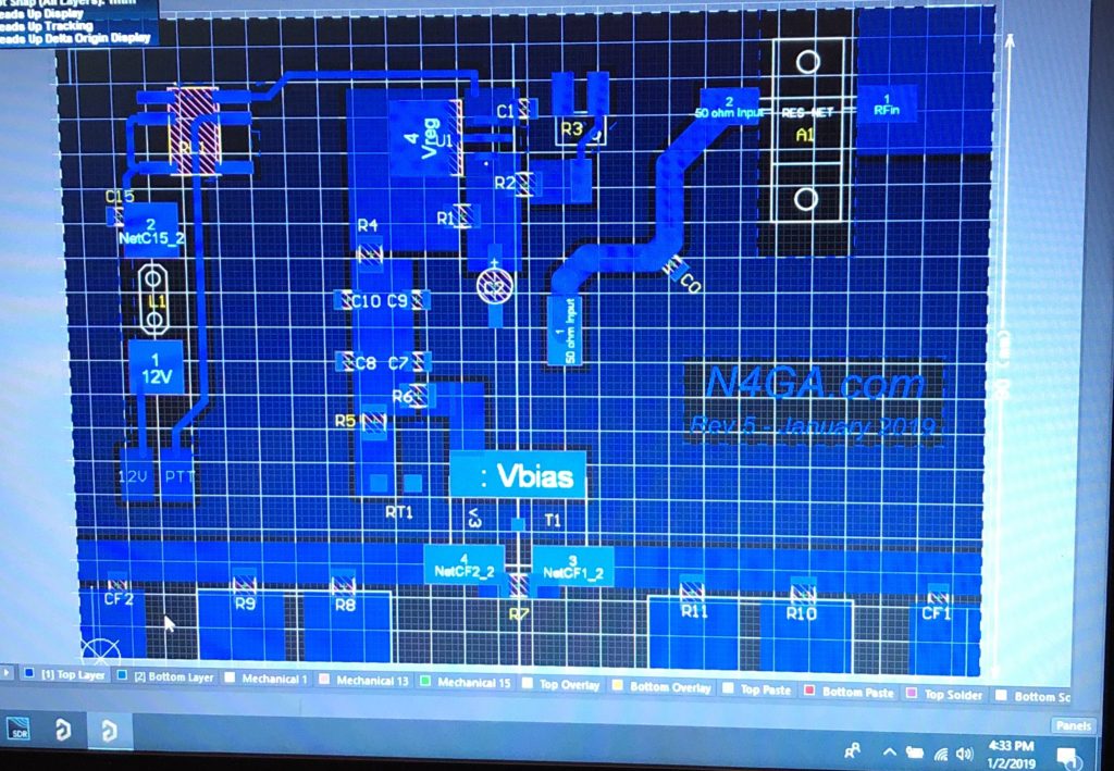
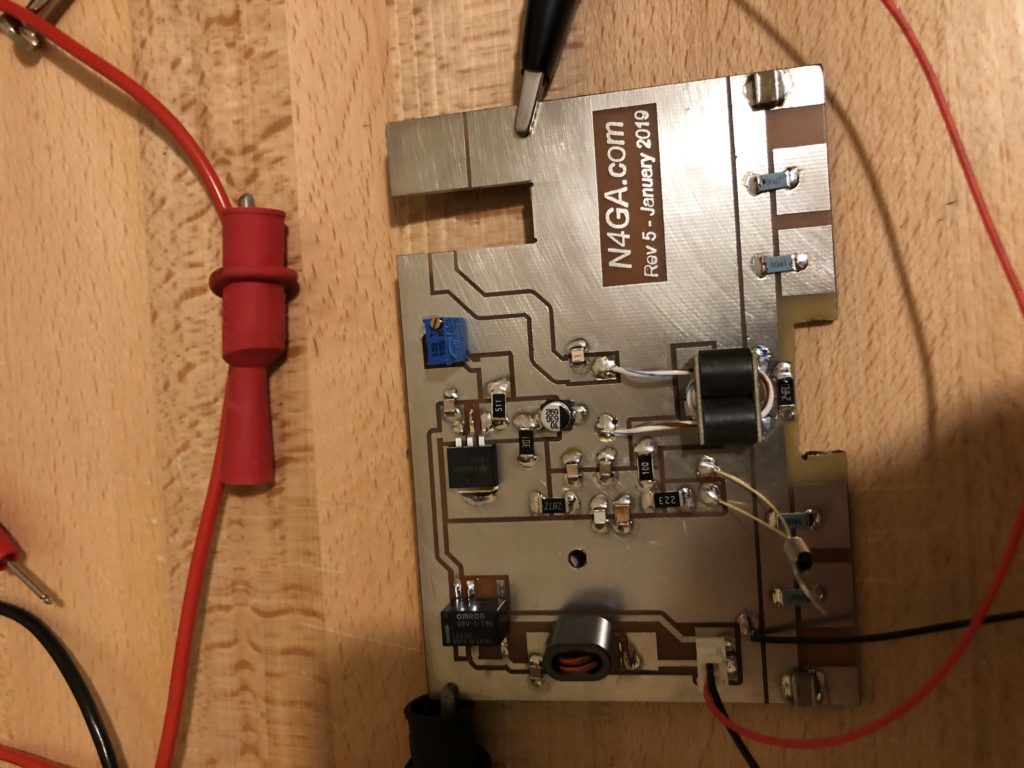
After a month or so of running SPICE simulations in my spare time (primarily while watching sports on TV), I arrived at a design using a LM317 adjustable regulator, a 5k NTC thermistor and a well chosen voltage divider network.

Voltage v Temp (in resulting resistance) of Thermistor

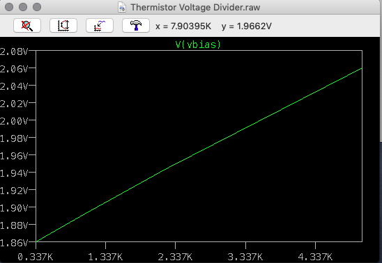
Nice thing is, the temp curve of a 5k NTC therm is linear so I could design around this. It all came down to scaling to get the bias adjustable in the tight little range required (~3 to 3.5V) while keeping the slope of the temperature adjustment curve at -2.5mV/degC.

So in layman’s terms: get the slope to -2.5mV/degC and center the curve at a specific voltage of ~3.25V. Fun little puzzle requiring a lot of .STEP and Monte Carlo in SPICE.

The new circuit is built and tested and works flawlessly. I can set the amp for 4A idle current at room temp, heat it up so hot you can’t even begin to touch the heat sink, and the idle current will still be 4A.

Mission Accomplished!

Also see related articles:

Single versus Dual Bias for LDMOS RF Amps

Nulling the Even Harmonics

2x LDMOS Bias Supply Front End

Comments

19 responses to “Biasing Schemes Revisited”

  1. Alan Anderson Avatar
    Alan Anderson

    I’m glad you went through this, I was about to change to the dual bias…now I can save that time. About ready to fire up the duals finally, reformatting the inside of the amp to get more air flow,

    Alan / KJ4BIX

  2. Steve Senft Avatar

    I’d love to see a full schematic with component values – and the part number for the thermistor!

    How well did this circuit null out the even harmonics? In my mind, that seems to be one advantage a dual bias supply potentially offers. Reducing every watt of power reflected back to the expensive FET(s) is doubtlessly a smart move.

    I’ve been lurking in the background for a while, and wondering what you are doing for a LPF?

    73 – Steve KG4LJB / C6AJB

    1. N4GA - Rob Avatar
      N4GA – Rob

      Steve, Sorry about the delay here. Didn’t know you posted this until I logged into the dashboard. Shoot me an email and I can get you the schematic. 73s

      1. OK2TSV Avatar
        OK2TSV

        Hello Rob,

        I would like to build the bias circuit as yours to my new 70cm LDMOS(MRFE6VP61K25H) PA. Could you please send me the schematics for the bias to my email?

        Thank you
        Best regards,
        Lada OK2TSV

        1. N4GA - Rob Avatar
          N4GA – Rob

          done

  3. Roger Klein VE3MVL Avatar
    Roger Klein VE3MVL

    Rob, nice job, I also have been lurking in the background for a Bias solution to come up. Have you published the schematic for all this hard work ? appreciate if you are making it available. I am an 80 year old back into the hobby after a busy 30 yr lapse. My only rig is a TS 590sg, so i am more less confined to 100w and low SWR.
    Amazed at; and fully appreciate all the refinements in the hobby in the last few years. My sleeves are rolled up in this catch-up phase of my life. I more or less left off with the Motorola RF handbook in the early ’80s
    Roger

    1. N4GA - Rob Avatar
      N4GA – Rob

      Roger – welcome back!!!

      Yes, in 30 years the amplifier technology has changed a lot, at least with respect to the solid state LDMOS devices available these days. Of course all the governing physics remain in effect! Ha ha

      And some of them got even more difficult, not less. Like dealing with 1500W in a 3 ohm impedance world. Lots of challenges of its own there.

      I’ll try to get a bias schematic posted. Not hiding them, its just that every one of them I make is a little different.

      73s!

  4. Roger Klein ve3mvl Avatar
    Roger Klein ve3mvl

    Yes, a challenge for the Gray Matter especially with the sweet new things out there for hams, I am all ears Rob. You speak of 3 ohms, Granberg was asking for less than that in the Motorola Rf handbook, I wound a few of his transformers with Stackpole material for the MRF’s , but quickly realized I was really an amateur dealing with the ring of fire. I still have them somewhere, but this LDMOS stuff looks mighty tasty. Thanks.

  5. Andy Wood Avatar
    Andy Wood

    Hi Rob,

    I have been lurking and watching your work for some time. I must say it is very impressive! I am about to embark on my dual device journey after completing a few single device models. Are you willing to share your bias circuit schematic with me via email?

    Regards,
    Andy VK4KY

    1. N4GA - Rob Avatar
      N4GA – Rob

      Andy,

      I will email it to you. I have several bias schemes I use and you have inspired me to do a separate post on bias schematics. But look for my email.

      73s!

  6. Brian Avatar
    Brian

    What do you think about the statement (page 5) from Ampleon… regarding the very low output impedance of the bias source?

    https://www.ampleon.com/dam/jcr:c2a56618-6652-4788-a33c-79019db73740/R_10032.pdf

    1. N4GA - Rob Avatar
      N4GA – Rob

      I’ve seen that comment in that doc. It’s also repeated in various solid state amp books. I’ve always viewed it as basically saying that the bias voltage needs to be “firm” and not easily affected by the RF voltage swings on the gate.

      So if you imagine this 2.6V being delivered to the gate through a low impedance (say 1 ohm) versus a high impedance (say 100k) which one will be more affected by current deviations? E=IR

      1. Brian Avatar
        Brian

        I certainly understand what they’re saying alright… and I adhere to that on all my bipolar amplifiers. High power bipolar devices have a very low input impedance for RF & DC. That’s why I feed my class-AB biasing for my bipolar amps via an emitter-follower with an output impedance of less than 1-Ohm. But the power MOSFET situation is quite different… it has a relatively low input impedance for RF… but very high impedance for DC. Since the bias is DC… I don’t really understand why a low impedance feed is needed for the power MOSFET bias source.

        1. N4GA - Rob Avatar
          N4GA – Rob

          The best way to clear your mind on this is to know that the kid who was tasked with writing that datasheet probably did what 90% of RF designers do – blatantly copy what happened before them.

          This happens in RF, everywhere and all the time. Crack open a brand new commercial RF amp. You’ll see rule-of-thumb practices in there that appear in 60 year old textbooks!

          Crap like 6 chip caps of varying values in parallel, used to ground RF.
          Crap like a large inductor in series with Vdd.
          Crap like a large electrolytic in parallel with Vdd.
          Junk like a Common Mode Feed Chokes with so much inductance that it’s effectively chocked off and you may as well not even have it.
          Feedback schemes that do nothing..

          On and on.

          1. Brian Avatar
            Brian

            Yes, I guess there are quite a few things said & done out there in the RF world that don’t make much sense, and are not checked before sharing. My opinion is… this statement from Ampleon is one of them. Thanks for your responses…

  7. Lonnie KL7U Avatar
    Lonnie KL7U

    Hi Rob,
    I just came across this while working up a bios supply for two MRE6VP61K25 circuits . . on the same heat sink as you said. I too would like to see how you stabilized the current. I also was thinking of dual bios.. Thanks for saving me the pain. Could you email me the circuit data please?
    Lon, KL7U

    1. N4GA - Rob Avatar
      N4GA – Rob

      Sent it, you get it?

  8. Brian - AD0UK Avatar
    Brian – AD0UK

    I would be interested in looking at your Schematics, and Parts list – I want to learn more about building this type of device and would greatly appreciate any help you can give as well.

  9. Steve Canfield K7SWC Avatar
    Steve Canfield K7SWC

    I’d bet you’re still very busy…
    you mentioned that you would do an article giving the bias circuits…
    will you possibly have time to do this in the future?
    thank you for all your contributions to the radio craft.

Leave a Reply

Your email address will not be published. Required fields are marked *