Single versus Dual Bias for LDMOS RF Amps

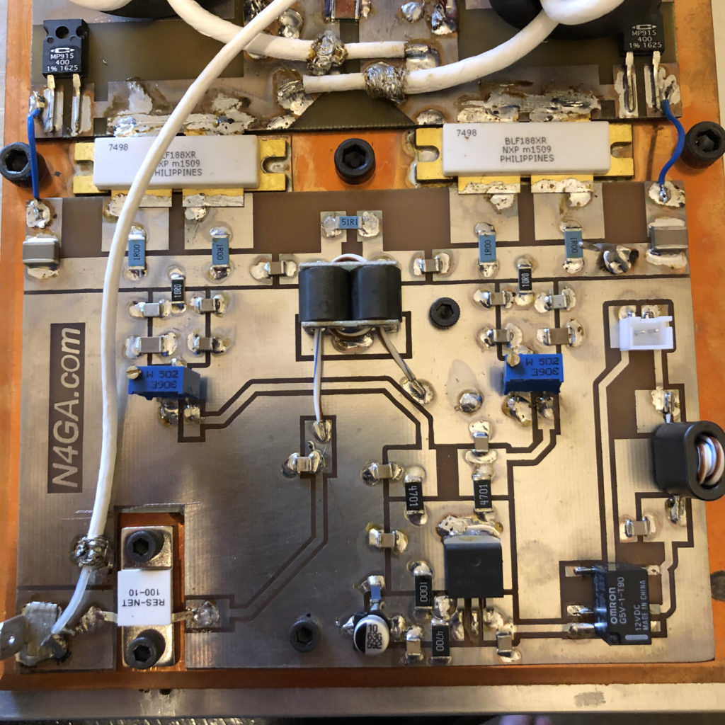
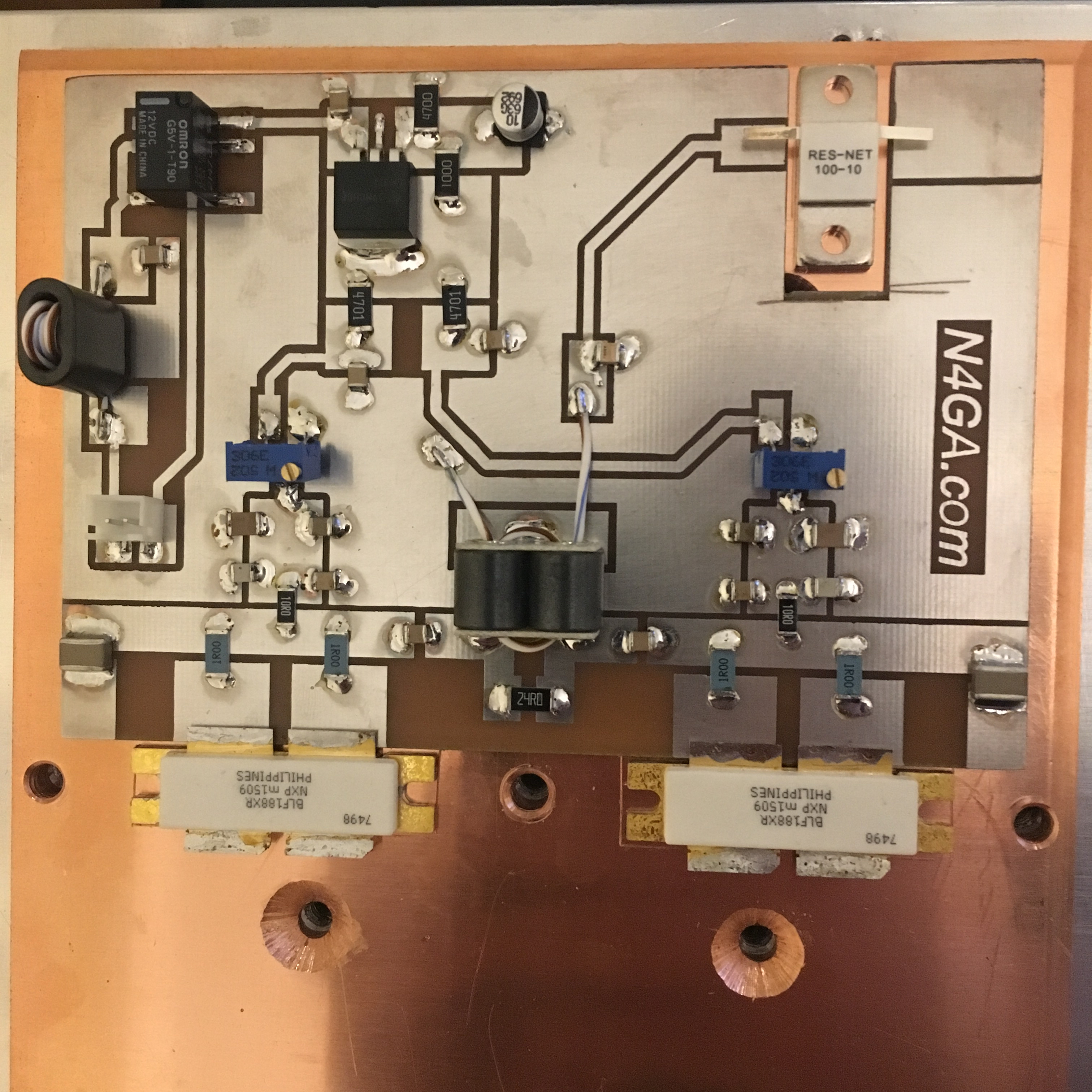
Last year I decided I would design and build a regulated temperature-compensated independently adjustable dual bias circuit for my 2x LDMOS amp. (what a mouthful)

Why? Because I wanted to try an experiment which actually works in a class AB audio amp. This being the ability to adjust the bias to affect the mix and magnitudes of even and odd harmonics.

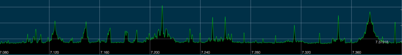
I wanted to see if this could be done in a class AB LDMOS RF amp and if so, to what degree. What I found was interesting but not all that useful. While you can adjust the biases to almost completely null out the even harmonics, not so surprising, you can not affect the odd harmonics more than a few dB.

There are many reasons for this. When you null harmonics in a AF class AB amplifier, you are primarily changing the crossover distortion profile, which in a AF class AB amp, is the key component to distortion.

In a RF amplifier, crossover distortion is not the target. There are other factors which are more limiting to the RF amp’s linearity. Some of which are:

  • extremely compromised, or non-existent CMFC
  • circuit stay inductances
  • LDMOS non-linearity

The first and third are the key. The second one can be managed well enough.

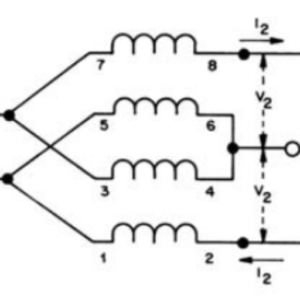
First, in a class AB RF amplifier, the job of the CMFC is to emulate a 1:1 center tapped transformer. However, it has to do this at RF, from 1-30Mhz, at power, and in a ridiculously low (1-3 ohm) impedance environment. It needs to do this with zero stray inductance, zero leakage inductance and near perfect mutual inductance. Again, from 1-30Mhz. That’s all it has to do!

Should be enough said about that. Not to mention, many designs don’t even have a CMFC!

Second, LDMOS non-linearity. Dig around on the internet until you find the equations for the generation of harmonics in a large LDMOS device. Insidious is the word that comes to mind. The other more boring term is NON-linear.

Back to the main topic…

The other thing I learned about a dual bias scheme is that it’s near impossible to get the initial bias set correctly. As soon as you begin, the amp instantaneously begins to warm up, so before you can get over to bank 2, you have a drift and compensation due to heat. So back and forth you go and you finally just try to get it “close enough” and give up.

This lead me to my final conclusion.

Since you can’t bias out the odd harmonics, you may as well go with a really good single bias. If you buy two devices together they will be sequential out of the fab and matched. Also, they will only be ~1.5 inches apart on the same piece of copper heat spreader and thus will be at the same temp. So a dual bias is not required!

Here’s the “really good” single bias.

Comments

12 responses to “Single versus Dual Bias for LDMOS RF Amps”

  1. Jay Alley, Jr Avatar

    Rob you are my hero!! I follow all your new post. You might say, I am one of you biggest design fans. I built one of your early designs. I think it was in 2017. It still works great. As I have related to you before, I am an old man(85), but still enjoy building, testing and tinkering(have a back ground in electrical engineering, the old stuff:):). I would like to know how you cut the foil on the circuit boards. They all look so neat and professional. Cheers!! Jay N4HD

    1. N4GA - Rob Avatar
      N4GA – Rob

      Jay – thank you for following the site and thank you very much for the nice words!!

      I make these PCBs in the basement using the old iron method. Some day I may do a little tutorial on the website but in short:

      1) Design the PCB in Altium Designer (PCB design software)
      2) Laser print this in a mirrored state onto glossy photo paper for a ink jet (so the laser toner [plastic] does not bond well with the paper)
      3) Iron this pattern onto the blank PCB
      4) Etch with hydrochloric acid + hydrogen peroxide mix
      5) Tin plate the PCB with some other chemical mix
      6) Drill all the holes
      7) Mount all the parts and blow it up and go back to #1

      🙂

  2. Sebastial Avatar
    Sebastial

    Hello Rob,
    As most AB push-pull amplifiers, even harmonics are practically zero, but odd harmonics are monsters and they come mainly from amplifier compression, not crossover. With a good negative feedback and keeping drain voltage swing within 85-90% of theoretical maximum swing (ie 1200-1300W PEP output @ 51,4V supply). Above this level, the sine wave will be compressed and odd harmonics will start to show. An extreme case will be in deep saturation near maximum theoretical power, where the output waveform will look qute trapezoid). Anyway, the harmonics will be trapped by the output Low Pass Filter.

    However there is also another kind of distortion, an this is IMD or Inter Modulation Distortion. BIAS current affects mostly IMD, and not harmonic distortion. IMD mostly known as splatter can not be filtered as IMD is actually a bunch of spurious emmisions around your transmission bandwidth. and can only be improved by means of BIAS, leading the device to work in a more linear zone. I suggest you use 1000mA of bias current for each half, ie 4000mA total bias current as each LDMOS has 2 halves.

    1. N4GA - Rob Avatar
      N4GA – Rob

      Seba,

      Really sorry your comment did not go through back on March 11! Very good info, much appreciated. Making sure it gets posted here for others to see.

      1. Frank Avatar
        Frank

        Hi,
        it is always a fight with physics. Some pcb programs deliver smooth shapes for RF.
        Looking at the image, got it. You don’t have any ground vias……

        1. N4GA - Rob Avatar
          N4GA – Rob

          Correct. Can’t make VIA’s at home. It’s a major pain and a major limitation.

  3. Brian Avatar

    I agree… dual bias is completely unnecessary… since the AB-bias level of the devices has almost no effect on harmonic content. I’ve designed a temperature-tracking bias circuit that uses a bipolar transistor (bolted directly to the heat sink) to track the sink temperature. I then use that signal piped into an op amp… to provide some fine-tuning to the 2mV/C temp drift of the MOSFETs. I’m able to hold the drain current to 5% of any bias value I set… from -20C to +100C sink temperature. This is more than adequate.

    1. N4GA - Rob Avatar
      N4GA – Rob

      Brian – thanks for the comments!

      The bias level of AB amp has a large impact on harmonics. As you approach zero, the amp is class B with a huge nasty crossover distortion. As you approach Vgs Max, the amp is a push pull class A amp with very little harmonic content, but not real practical at high power levels (think 40A Ids idle…lol).

      Having a dual bias lets you control each side individually and this too could be good for like an audio amp. What I found with these high power LDMOS amps is you can “customize” the harmonics, with a dual bias. But when you do, you basically just redistribute. So if you lower say your 3rd by 10dB that pops up the 2nd by nearly the same. Call it conservation of harmonics. ha ha

      I think the main reason is these gemini devices, like the BLF188, are pretty darn well matched. If these were two discrete devices with significantly different characteristics, a dual bias might be very beneficial, so you could attempt to match them…at least at a specific power level.

      Yes, using a BJT to track the temp is good. You can also use just a diode (same p-n junction). You could also use the exact same material as the output device for a perfect match – but that might get costly!

      Lots of effective bias circuits out there. My current favorite is floating a 5V regulator on top of a diode and using the diode as the temp sensor to drop the voltage of the entire regulator. That said, the ultra simple NTC Therm and a simple resistor voltage divider circuit works quite well too.

      1. Brian Avatar

        From my experience, I haven’t had much luck getting all of the harmonics below what I consider an acceptable level (-36dBC)… without some filtering on the amp output.

        1. N4GA - Rob Avatar
          N4GA – Rob

          It’s a fight with Physics..

  4. Amilcar Carlos Avatar
    Amilcar Carlos

    Rob, I had build in years a two VRF157 amplifier and now change it for a MRF 1k50 flange w screws. 1Kw 1-60Mhz.
    What are the best Bias current for operation im SSB AB classs?
    And it can be soldered to the cooper or flange screw ?

    Thanks

    CT1TO – Amilcar

    1. N4GA - Rob Avatar
      N4GA – Rob

      A good bias is ~1A per device, so 2A total for a dual device amplifier.

      The devices can be soldered or screwed down. I solder mine down, so there’s little question about the thermal conductivity.

      73s! Rob N4GA

Leave a Reply

Your email address will not be published. Required fields are marked *